Low-Tg: The Fiasco Behind Massive GPU Failures
A look back at the engineering errors that led to the appearance of "bumpgate" in NVIDIA and ATI GPUs in laptops and certain gaming consoles such as the PlayStation 3 with the Yellow Light of Death (YLOD) and the Xbox 360 with the Red Ring of Death.
Revisiting the feared "bumpgate"
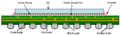

Diagram of the main GPU chip showing the die and the substrate, and between them, the underfill layer which joins them together through solder joints. Image courtesy of GPU reflow guide, VAIO Library.
The main packaged silicon of a graphics processing unit (GPU) of a graphics card can be divided into two layers with an intermediate layer that electrically communicates between them through metal solder joints enclosed within a semi-rigid underfill layer. Underfill is typically a layer of thermosetting epoxy resin with a high content of silicon oxide particles, providing a low coefficient of thermal expansion and high elasticity, making it flawless for permanently bonding the substrate to the die without cracking, as well as reducing the mechanical stress to which the solder joints are subjected with thermal cycles. It arose from the invention of flip-chip packaging technology, which emerged due to the limitations that traditional packaging had for accommodating a large number of transistors and diodes.
IBM patented it in the early 1960s and used it primarily for its mainframes. They later developed Controlled-Collapse Chip Connection (C4), which connected the die to the substrate via tiny solder joints made of a lead-rich alloy, and which would be commercially released in the Solid Logic Technology (SLT) modules launched in 1964 for the IBM System/360 mainframe computers. At first glance, it was not quite as flip-chip as today's processors are, as they still had clumsily soldered copper balls and so the term "flip-chip" was not coined by IBM but by DEC. However, subsequent work by IBM, DEC and Motorola would eventually engender to the adoption of the flip-chip as a standard in the production of VLSI CPUs, which used underfill solder joints made of a lead-rich alloy, that is to say, 97% lead (Pb) and 3% tin (Sn).
The invention of flip-chip packaging technology came very early, so much so that it occurred just a few years after Jack Kilby, William Shockley, Robert Noyce, and Walter Brattain patented their discoveries. At the time, wire-bonded packaging technology was the most widely used, and it continued to be used for the next 30 years, with the number of transistors reaching one million in 1990 with the Intel 80486, whereas flip-chip packaging technology, which had numerous advantages over wire-bonding packaging technology, stagnated.
This is due to the fact that silicon packaged using flip-chip technology has a low coefficient of thermal expansion, which, as previously mentioned, is approximately 2.5–3 ppm/C. To ensure their survival under the thermomechanical fatigue they are subjected to during operation, they had to be assembled on more expensive ceramic substrates than traditional FR-4 or BT-Epoxy (Bismaleimide-Triazine) substrates, which were often up to 10 times cheaper. Flip-chip packaging technology was rarely used for the production of VLSI-based integrated circuits such as CPUs until Intel brought it back in 1999 with the introduction of the Pentium III (codenamed "Coppermine").
The ugly thing about Low-Tg underfill
Years earlier in 1984, Hitachi developed highly thermosetting epoxy resin underfill materials with applications that could potentially help reduce thermomechanical stress on the solder joints that electrically connect the substrate to the silicon die, and so it was. In addition to bringing back flip-chip packaging technology as we know it today as FC-PGA (Flip-Chip Pin Grid Array), the classic ceramic substrate was replaced by an organic laminate substrate, although it has superior electrical performance, it has a higher coefficient of thermal expansion compared to the silicon die. This subjected the solder joints to greater mechanical stress than they would be if the substrate were ceramic.
Intel could have solved this problem by using the invention of thermosetting epoxy resin underfill materials developed in Hitachi's Japanese laboratories in 1984, were it not for the fact that the rise of laptops posed a problem for High-Tg resin, as its rigidity offered little absorption against knocks or falls, transferring that force of impact to the solder joints, which despite using a lead-rich alloy, with 95% lead (Pb) and 5% tin (Sn), were so small that only a few impacts would be enough for the CPU to fail, giving rise to a concerning reliability problem.
A high-Tg epoxy resin encapsulating the solder joints that electrically connect the organic laminate substrate to the silicon die also appeared to conflict with current solutions to signal delay as microprocessors became more miniaturized and their internal connections moved closer together, causing both capacitance (C) and resistance (R) to increase due to an ever-increasing time constant (RC). Although this internal wiring was made almost entirely of copper, it still presented some resistance to the passage of electrons like almost any other electrically conductive metal, and as the internal wiring became more miniaturized, the resistance, measured in ohms (Ω), increased.
Intel employed an elegant solution to this: kicking the problem down to the packaging technology level. They introduced silicon dioxide (SiO2) as a low-K (dielectric constant) dielectric from their processors manufactured at a 90-nanometer technology node and since the delay of electrical signals is directly proportional to the product of both the capacitance and the resistance, then the reduction of the first variable (C) implies a reduction of the second variable (R). This partially solved the delay in electrical signals, improving performance.
With the inclusion of silicon dioxide (SiO2) as a low-K dielectric with porosity, a new problem arose due to the resulting mechanical fragility, since the present High-Tg used in the underfill layer between the substrate and the silicon die did not provide sufficient absorption against impacts or blows, owing to the fact that this material has porosity and is not very dense, it tended to break under unfavorable mechanical conditions. Faced with this conundrum, it was decided to use a more rubbery underfill (low-Tg), with greater impact absorption capacity, but with less capacity to counteract expansion and contraction under thermal stress conditions, leaving open a concerning reliability problem.
Although this problem was left open, it seemed that the solution was already given on the side of the solder alloy used for the joints between the substrate and the silicon die, since it usually contained a moderate amount of lead (37%) and even a high amount of up to 95%, which provided sufficient resistance to mechanical stress to cause significant reliability problems. As such, the use of Low-Tg was only compatible and viable to the extent that lead-containing solders were used for solder joints due to their resistance to mechanical stress, not with lead-free solder alloys, which tended to crack more frequently, all else being equal, than lead-containing solder alloys.
Despite lead's resistance to mechanical and thermal stress, which makes it useful in countless industrial applications, it is just as useful as it is toxic, capable of seriously affecting almost any organ in the human body even in tiny concentrations. "There is almost no function in the human body that is not affected by lead toxicity," concludes the abstract of a study that reviewed the toxicity of lead throughout history, highlighting the consequences of its past use as an anti-knock additive for gasoline in the form of tetraethyl lead,1 an extremely toxic and potentially fatal substance even at low concentrations that lowered the IQ of Americans due to its devastating effects on the brain.
Lead-free solder, although it still contains heavy metals such as silver, is not as toxic or polluting as lead-based solder. Despite this, it is not as malleable or wettable as its lead-containing counterpart. Its melting point of 217-221°C makes it more susceptible to fracture under thermal and mechanical stress conditions, such as those seen in graphics cards, where solder joints must electrically communicate the substrate — with a higher coefficient of thermal expansion — to the more stable silicon die with a coefficient of around 2.5-3 ppm/°C.
Due to its toxicity, lead began to be considered a highly polluting heavy metal on a par with mercury and cadmium, whose use should be strictly restricted to those applications where it is absolutely necessary in the absence of alternatives with equally satisfactory properties. The introduction of the RoHS (Restriction of Hazardous Substances) directive, a.k.a. "2002/95/EC", introduced in the European Union on January 27, 2003, enforced on February 13, 2003, and made mandatory on July 1, 2006 for all electronic products circulating in the European Union market, imposed severe restrictions on the use of toxic heavy metals such as cadmium, mercury, and lead. The regulation also provided exceptions to the veto in fields where certain materials are deemed essential due to their unique and unreplicable properties.
Regardless of these exceptions, the European Union did not consider granting one for the electronics industry, where — given the extreme toxicity and danger posed by lead — alternatives to lead-containing alloys had already been investigated until at least a decade before the prohibitions imposed by the new regulation that would take effect on July 1, 2006. Years earlier, as far as is known, a lead-free eutectic solder alloy was first synthesized at Ames National Laboratory in Iowa by Iver Anderson, John Smith, Chad Miller, and Robert Terpstra, with a co-inventor, Frederick Yost, at Sandia National Laboratory, between 1992 and 1994. This ternary formulation consisted of tin (Sn), silver (Ag) and copper (Cu), with an approximate melting point of 217°C (or 422.6°F), and was made public in 1995 under patent US5527628A.
The present day, it can be asserted that this family of solder alloys are as resistant to tensile stress as alloys made of lead (Pb) and tin (Sn), despite being more expensive and including more additives than the eutectic alloy of yesteryear. Moreover, surface-mount methods using a ball grid array (BGA) have been refined for flip-chip packaging, and a red adhesive is now introduced during the assembly process around the package to reduce the thermomechanical stress on the solder joints that electrically connect the entire chip to the printed circuit board, preventing premature failures due to communication paths to the chip without electrical continuity due to broken solder joints.
But in those years this was not the case. When the regulation was introduced as a mandatory requirement for all goods traded within the European Union, the solder alloy consisting of tin (Sn), silver (Ag), and copper (Cu) was in a very immature state. Not only was it more brittle than lead-containing alloy, but it was also much less ductile, malleable, and wettable, making it even prone to generate short-circuits through bridges with adjacent joints, which also happened with some NVIDIA or ATI GPUs that used the immature lead-free solder alloy formulations consisting of tin (Sn), silver (Ag) and copper (Cu), resulting in short circuits that are unrepairable as they occur inside the chip.
As a result of the inclusion of a solder alloy that is very disadvantaged compared to the lead-containing counterpart, what happened most often were not fatal short-circuits caused by bridges between solder joints, but broken solder joints due to continuous thermomechanical stress. It turns out that the accelerated adoption of the more fragile lead-free solder alloy was not accompanied by a corresponding refinement of the materials used in the underfill layer. As previously mentioned, solder joints are added during the wafer bumping process in flip-chip packaging, and the underfill is applied and sealed after the die has been singulated and attached to the substrate.
In summary, the underfill with a low glass transition temperature (Low-Tg) was maintained even when lead-free solder alloy began to be used for the solder joints between the substrate and the silicon die, thus forcing the already gummy underfill to protect solder joints that are less mechanically resilient than they would otherwise be if they were made from an alloy consisting of lead and tin. Perhaps NVIDIA and ATI, guided by the aphorism "If it works, don't fix it," remained reticent to dare to touch underfill, whose formulation used at the time seemed to be bullet-proof, which proved to be an absolutely ruinous and disastrous engineering decision, even for those years.
The painful adoption of lead-free solder alloy
In anticipation of the already announced mandatory introduction of the RoHS directive, which would end up materializing officially on June 1, 2006 in all electronic products traded within the European Union market, a year earlier several companies — including NVIDIA and ATI — began to include lead-free solder for electronic products that required it. Since then, the formulation frequently used for solder joints between the substrate and the silicon die consisted of tin (Sn), silver (Ag) and copper (Cu), with a little more or a little less of each of the aforementioned elements. The solder joints of surface-mounted integrated circuits with a ball grid array would be made of a lead-free alloy.

In line with the above, ATI agreed to co-design with Microsoft the GPU that would be included in the successor to the first-generation Xbox, whose GPU was NVIDIA's NV2A based on the "Kelvin" architecture with a 150-nanometer manufacturing process. This led to the creation of the Xenos, which from the Y1 revision (codenamed "C1") to the Vejle revision developed in mid-2010 that reformed it to make it a system-on-chip with CPU and GPU in a single package, included the eDRAM (Embedded DRAM) — produced by NEC — in the same flip-chip, resulting in a multi-chip package with 2 silicon dies on the surface, thus reducing the latency of the exchange of electrical signals.2
The classic Xbox launched in 2001 brought with it a forcefully bulky, aggressive, very "American" and poorly portable design. It weighed 4 kilograms (8.6 lb), compared to the 2.2 kilograms (5.0 lb) offered by Sony's PlayStation 2 at the time, which would be reduced to just 0.9 kilograms (2.1 lb) with the introduction of the Slim version in 2004. The design language of the classic Xbox went against the grain of what companies like Sony were pushing with their commitment to lighter, more minimalist, and cleaner designs, ergo favoring sales of the PlayStation 2 to the detriment of the classic Xbox, which performed very poorly in terms of sales in countries like Japan.
For this reason, Microsoft bet for a minimalist industrial design language for the Xbox 360. In the first revision of the console known as "Xenon" — not to be confused with the CPU of the same name — they introduced a cooling system that involved the use of aluminum fins and copper pipes that thermally conducted the heat generated by the CPU for subsequent expulsion by the fan, something that the GPU did not enjoy, having to work with an aluminum-only heatsink, which did not help conduct heat as well as copper piping would.
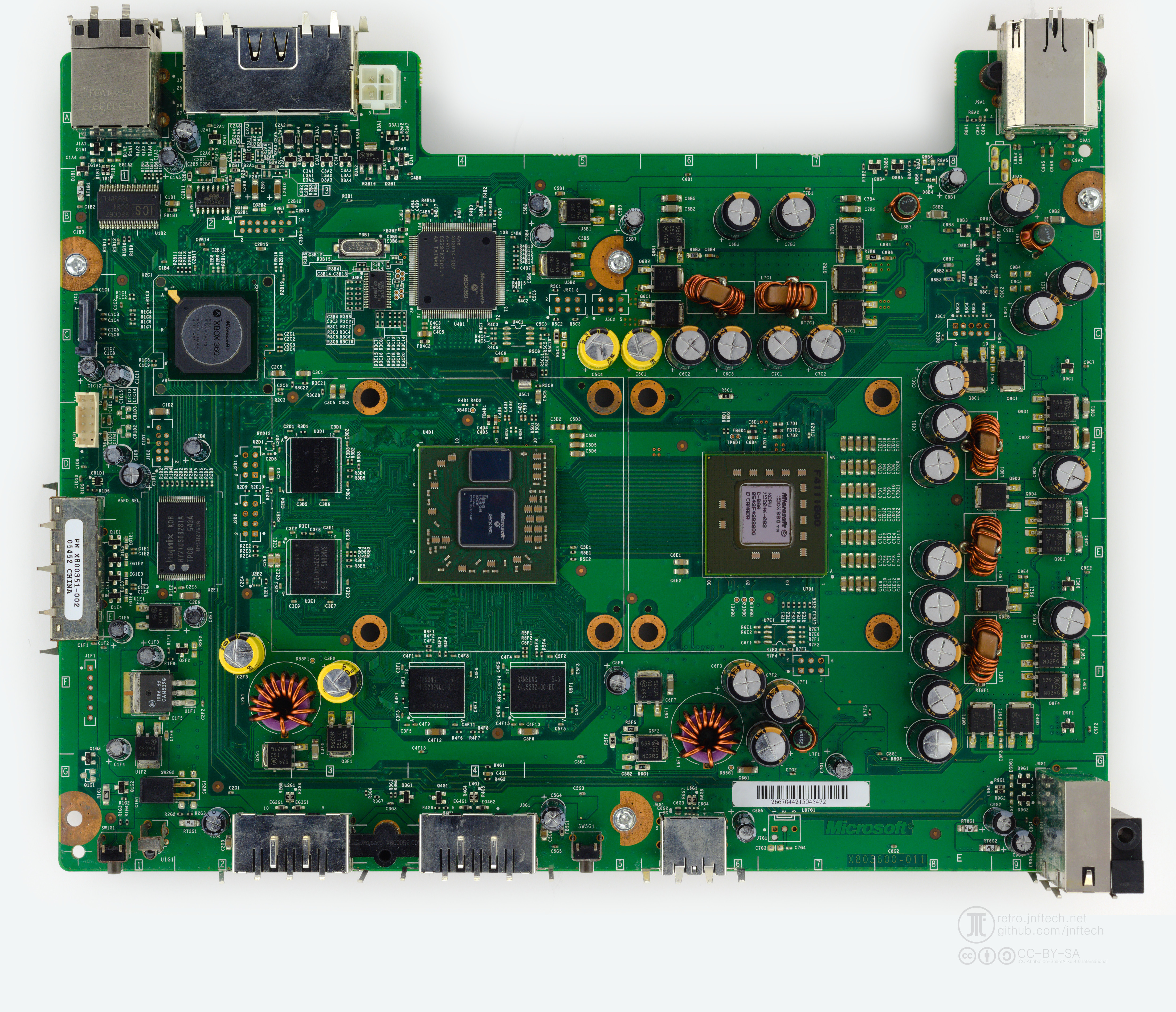

Final version of the motherboard for the "Xenon" revision of the Xbox 360 under the part number "X803600-011". Image taken from Xenon (Motherboard), XenonLibrary.
The ATI's "Xenos" GPU — based on the ATI Radeon X1900 — and IBM's "Xenon" CPU were based on a 90-nanometer manufacturing node process. Microsoft and IBM agreed to choose this manufacturing node as a way to cut production costs with the aim to make the Xbox 360 more competitive with Sony's PlayStation 3, launched on November 11, 2006, in view of the fact that more advanced manufacturing nodes such as the 65 nanometer one already used by Intel for the production of the Pentium D (codenamed "Presler") were much more expensive, resulting in a silicon with more capacitance per transistor given its feature size, less energy efficient, and with greater heat generation.
In conjunction with this, for ATI's Y1 revision "Xenos" GPU, solder joints made of tin (Sn), silver (Ag), and copper (Cu) were included in the wafer, and the underfill with a low glass transition temperature (low-Tg) formulation was maintained. This formulation, previously considered "bullet-proof", tended to become rubbery when subjected to high temperatures, which left the wafer solder joints unprotected from the thermomechanical stress of expansion and contraction of a substrate with a relatively higher coefficient of thermal expansion than the silicon die. In compliance with the new directive, NVIDIA introduced the GeForce 8 series (codenamed "G8x") on November 8, 2006, also featuring a lead-free solder alloy in the wafer solder joints, as well as in the solder joints that attach the flip-chip to the printed circuit board.
The bubble bursts
In May 2005, the Xbox 360 was unveiled at "MTV Presents: The Next Generation Xbox Revealed", and was officially released on November 22, 2005, even though it was known within Microsoft that they were close to producing an inherently faulty product. Despite factory reliability tests showing that the Xbox 360 had a high propensity to eventually fail, this did not stop Microsoft from continuing production, as they sought to have a video game console on the market before the launch of Sony's next console as a way for it to outsell the PlayStation 3.
Subsequently, Microsoft decided to add a hard drive bay in a hasty redesign of the "Xenon" revision of the Xbox 360 that also introduced wireless controllers, further compromising the airflow of a product that — as revealed in a memo dated August 30, 2005 — suffered from problems such as solder joint breakage due to thermal cycling, quality issues with VRAM (Infineon or Qimonda), and a DVD drive that could scratch the surface of optical discs, permanently damaging them. Despite such problems, it was decided that production would continue.
For the production of the Xbox 360, Microsoft subcontracted the American company Flextronics and the Taiwanese company Wistron, who were in charge of producing it through their factories located in China, who reported that the production yield of the Xbox 360 — the number of functional units that left the factories — was low, since by August 2005 the failure rate reached the not exactly modest percentage of 68%, contributing to Microsoft having difficulty meeting the high demand for units due to a lack of sufficient functional units.
In August 2005, an engineer said, "Stop. You have to shut down the line." It was widely known within Microsoft that what was being produced was a time bomb, but production could neither be postponed nor stopped. On November 22, 2005, the Xbox 360 was officially launched in North America and its commercial performance was excellent, at least in the United States, where it turned out to be the best-selling video game console until June 2008, when it was surpassed by the Wii. But Microsoft received reports, which they described as "isolated," about consoles that failed immediately after the purchase, and to which Microsoft would respond by extending the warranty to 3 years.

At the end of March 2006, the situation was beginning to slide toward complete unsustainability, as Microsoft, despite having shipped more than 3.3 million units, still had a growing pile of 600,000 failed units at a Wistron facility and at repair centers located in Texas, whether defective products that failed during reliability testing conducted at manufacturing facilities or returned defective units.3 Such was the unreliability of the Xbox 360 that people like Chris Szarek, a then 37-year-old photographer from Massachusetts, had four failed consoles, and he felt Microsoft was disrespecting him as a result of ignoring his complaints. In response, Microsoft calmed customer discontent with faulty units by increasing production to meet growing demand for working units and to serve those affected by the shortage.
In parallel to such a disaster, NVIDIA was having problems with Apple. On November 8, 2006, they introduced the 8-series (codenamed "G8x") of their GeForce GPUs — the first to feature CUDA — based on the "Tesla" architecture and supplied them to manufacturers such as Sony, Acer, Asus, Apple, Hewlett-Packard, and Dell to graphically enhance their devices.
But as a result of these poor engineering decisions, absolutely nothing went right. Apple's MacBooks produced between May 2007 and September 2008, both the 15-inch and 17-inch models, exhibited a high propensity for premature failure, which was quickly identified as being caused by the NVIDIA GeForce 8600M GT it came equipped with. Dell's XPS M1530 — also powered by an NVIDIA GeForce 8600M GT — was affected, with customers reporting that their unit failed completely just three months after purchase. Sony Vaio products such as the VGN-AR, VGN-FZ, VGN-NR, VGN-SZ and the VGX-TP were also affected, as were several HP Pavilion and Compaq models.
As evidenced in the litigation documents in the class-action lawsuit filed against NVIDIA for knowingly supplying defective GPUs and refusing to take responsibility, it was well-known within the company since late 2006 that GeForce 8-series GPUs exhibited a high failure rate due to breaks in the solder joints between the substrate and the silicon die of the flip-chip as a result of thermal cycling, as identified by Hewlett-Packard engineers in 2007 after receiving numerous complaints of defective devices in cases involving discrete GPUs from NVIDIA and ATI.
Far from what one might think, the culprit in this case was not the lead-free solder alloy, but the lead-rich solder alloy. The somewhat vague explanation provided in the aforementioned document alleges that NVIDIA observed that "solder bumps" (solder joints) placed on the substrate prior to packaging dicing cracked when subjected to pressure testing. These solder joints were made of the traditional eutectic solder alloy of 37% lead and 63% tin until NVIDIA observed problems in pressure testing and decided to substitute it — in a clearly erratic and hasty decision — with a lead-rich solder alloy, up to > 90% lead. This lead-rich solder alloy exhibited a high melting point of > 300°C and high rigidity, resulting in lower resistance to thermomechanical stress (tensile) than its eutectic counterpart with a moderate amount of lead.
This tensile stress, resulting from the thermomechanical stress that the solder joints must withstand without breaking, is caused by the mismatch in coefficients of thermal expansion (CTE) between the silicon die and the packaging substrate as the flip-chip expands when powered on and contracts when powered off. This requires a well-formulated alloy such as the traditional eutectic that adds tin to improve tensile strength reaching ~5.13 ksi (35.4 MPa) which with lead alone would be an insufficient ~1.74-2.47 ksi (12-17 MPa). Lead provides wettability, malleability, and softness, while tin provides resistance to mechanical stress, thus providing greater long-term reliability.
In applications where sustained temperatures around 200°C are expected, the use of a lead-rich solder alloy with a melting point of ≥ 300°C would be justified since the operating temperature exceeds the melting point of 183°C of the aforementioned eutectic solder alloy, but that is not convenient for an application where the expected operating temperatures are 50-100°C which places them far from the 300°C melting point of a lead-rich solder alloy. The reason for such a dilemma is given by what is commonly referred to as homologous temperature, which establishes a calculable ratio between the operating temperature and the melting point, which extrapolated to an electronic circuit suggests that it operates at only a fraction of the temperature corresponding to the melting point of the metal alloy used in solder joints.
To calculate this ratio by expressing temperatures in Kelvin (K), we can assume that the operating temperature is 50°C and then take the value corresponding to the melting point of the eutectic alloy with 63% tin and 37% lead (183°C).
We will obtain that the homologous temperature is (very homologous), and what would happen if we assume that the melting point is 327°C understanding that the lead-rich solder alloy used contains 95% lead and 5% tin? A less homologous temperature of .
In a January 1987 benchmark conducted by researchers at the Department of Materials Science and Mineral Engineering and the Lawrence Berkeley Laboratory at the University of California, Berkeley, it was found that a lead-rich solder alloy consisting of 95% lead and 5% tin with an approximate melting point of 327.5°C, under thermal cycling between -55°C and 125°C, saw extensive cracking occur earlier than its eutectic counterpart consisting of 60% tin and 40% lead.4 This further underscores the unusual nature of NVIDIA's decision to shift to using a lead-rich solder alloy in an application where expected temperatures of 50-125°C are poorly homologous to the 300°C melting point.
Although machines equipped with GeForce 8-series discrete graphics tended to fail up to 40% of the time at some point after purchase, NVIDIA did not fully accept responsibility, refusing to do so even when Apple engineers identified the graphics cards they were being supplied by NVIDIA as the sole cause. Apple decided to absorb all costs and responsibility for repairs to defective units even if the warranty for them had expired, which did not please Steve Jobs at all, who turned Apple towards ATI's discrete GPUs as a way of distancing from NVIDIA due to the lack of commitment they showed in even cooperating in identifying the fault and the costs that repairs would involve.
The symptomatology did not vary much among the computers affected by this defect: the complete failure — characterized by a black screen — was preceded by constant graphical and visual artifacts, glitches, performance issues, crashes, and apparent problems easily confused with a faulty screen or a defective flat flex cable. As a result of these machines completely prescinds from integrated graphics and rely entirely on discrete graphics for their graphic rendering, it was not possible to switch to alternative graphics that would allow the machine to continue functioning in the absence of functional discrete graphics, leaving the machine completely unusable.
It was a relief that the units produced with only the modest integrated graphics from Intel, such as the GMA 950, GMA X3100 or GMA X4500, were not affected by this manufacturing flaw, perhaps resulting in a boost in sales for machines with integrated graphics from Intel, but to the detriment of sales of machines with unreliable discrete graphics from NVIDIA or ATI. Years earlier, ATI was involved in the Red Ring of Death (RROD) failure on the Xbox 360 "Xenon" motherboard by supplying faulty graphics cards to Microsoft, who continued production of an unreliable product that, according to internal estimates, failed completely in up to 68% of cases. It did not even pass factory reliability tests.
As a temporary solution, Dell extended the warranty to 5 years, covering only those units that were defective due to a faulty GPU by replacing the entire motherboard and issued a BIOS update (A08) for the XPS M1530 that kept the fans running at a higher speed than usual as a way to mitigate thermal stress, although without successful results, as the issue originated from the GPU as such. On the other hand, Apple, who is not a customer-friendly company, offered "free of charge" repairs even if the product warranty had expired for the 15-inch and 17-inch MacBook Pro with the NVIDIA GeForce 8600M GT produced between May 2007 and September 2008, at the same time as explicitly acknowledging the unusually high rate of premature failure and poor reliability of the defective models based on NVIDIA discrete graphics.
In July 2008, NVIDIA publicly acknowledged a higher than normal failure rate for some of their graphics processors due to a packaging defect. At that same time, NVIDIA assured Apple that Mac computers with these graphics processors were not affected. However, after an Apple-led investigation, Apple has determined that some MacBook Pro computers with the NVIDIA GeForce 8600M GT graphics processor may be affected. If the NVIDIA graphics processor in your MacBook Pro has failed, or fails within two years of the original date of purchase, a repair will be done free of charge, even if your MacBook Pro is out of warranty.5
In the meantime, Microsoft was dealing with the titanic problem that the Red Ring of Death was posing on the Xbox 360 and that would turn out to be a financial hemorrhage for them. The strategy of cutting production costs even where it is not advisable at all proved to be counterproductive for a product that, as more units were sold, more were returned. "There were so many problems, you didn't know what was wrong," one engineer told The Guardian about it, contradicting Robert Bach — President of Microsoft's Entertainment and Devices Division — who assured that the team of engineers in charge of testing the product were confident that it was ready for launch.
What was happening was a problem whose origin lay in the lead-free solder alloy, which at that time was very weak compared to its lead-containing counterpart. The solder joints located between the substrate and the silicon die of the flip-chip package were fracturing as a result of a low glass transition temperature underfill, resulting in a domino effect where the breaking of more solder joints resulted in the breaking of even more solder joints due to the reduced adhesion between the two pieces of the package. This series of events resulted in the transfer of such stress to the solder joints of the ball grid array commonly used in surface mount flip-chip packaging, giving rise to the same problems mentioned above. If you were lucky, the solution to this was to re-ball the ball grid array underneath the packaging.
In September 2006, Microsoft acknowledged that Xbox consoles produced in early 2005 were not delivering the expected quality and in an effort to safeguard the already damaged reputation of the Xbox brand, Microsoft publicly acknowledged the problem in July 2007 through Peter Moore — who advocated a return and replacement program for affected units — by providing warranty extensions after the cause of the failure was identified: a low glass transition temperature underfill. Microsoft did not reveal the causes behind the Red Ring of Death until the release of a 2021 six-part documentary in which they recounted how the use of low-Tg underfill led to the premature cracking of solder joints in the "Y1" (codenamed "C1") and "Y2" (codenamed "C2") revisions of ATI's "Xenos" GPUs. This problem was aggravated by the use of the problematic lead-free solder alloy, which proved incompatible with the low-Tg underfill formulation due to its increased brittleness.
ATI and Microsoft paused production of the "Xenos" sometime in 2008 and reinitialized production of a revised "Xenos" known as "Rhea" (codenamed "Y2.5") for the mounting in the "Zephyr_C" and "Falcon" revisions of the Xbox 360 motherboards. Initially, this revision of ATI's "Xenos" GPU, identified as the "X810480", remained as unreliable as its predecessors, continuing to use a low-Tg underfill formulation until the "X816970" version was introduced which used a high-Tg, more robust, less rubbery, and consequently more durable formulation. In mid-2009, variants of the "Rhea" were also produced in the "X810480" version with High-Tg underfill, which extinguished the reliability issues that ATI's "Xenos" GPU had been carrying over since the Y1 and Y2 revisions typically mounted on the "Xenon" revision of the Xbox 360.
This led to the unreliable revisions of ATI's "Xenos" GPU such as revision "Y1" and "Y2" being dropped in favor of "Y2.5" also known as "Rhea", which in versions identified with the part number "X816970" or "X816971" became considerably more reliable. These revisions included a more robust high-Tg underfill, and some of them are marked on the silicon die with "Htg85" or "Htg130" indicating that they contain a high-Tg underfill. Moreover, these revisions of ATI's "Xenos" GPU were typically installed on affected Xbox 360 motherboards as part of the repair program conducted by Microsoft for units affected by the defect, with the aim of returning to the customer a console that will not fail in the long term. This repair program did not include the use of reflow, a highly discouraged method that only provides a temporary and short-term solution, as the units that were subjected to it are only expected to last a few months or even weeks before failing again.
Separately, NVIDIA plans to take a one-time charge from 150 million dollars to 200 million dollars against cost of revenue for the second quarter to cover anticipated warranty, repair, return, replacement and other costs and expenses, arising from a weak die/packaging material set in certain versions of its previous generation GPU and MCP products used in notebook systems. Certain notebook configurations with GPUs and MCPs manufactured with a certain die/packaging material set are failing in the field at higher than normal rates. To date, abnormal failure rates with systems other than certain notebook systems have not been seen. NVIDIA has initiated discussions with its supply chain regarding this material set issue and the Company will also seek to access insurance coverage for this matter.6
The Red Ring of Death proved to be financially disastrous for Microsoft, costing it up to 1 billion dollars in a program intended to safeguard the already damaged Xbox brand. NVIDIA's refusal to acknowledge its central role in the "bumpgate" scandal, primarily associated with GeForce 8-series and certain Quadro graphics cards, led to a class-action lawsuit headed by Apple, Dell, and HP, which concluded with NVIDIA agreeing to pay out between 150 million dollars and 200 million dollars in refunds and repairs to affected units, covering advance warranties. Beginning in 2009, NVIDIA GPUs began to feature high-Tg underfill and a much more reliable lead-free solder alloy.
Final thoughts
The industry's immediate response to the subsequent fiasco caused by the use of underfills with a low glass transition temperature was to discontinue them for the purpose of prevent delamination between the substrate and the silicon die in packaging with flip-chip technology, prompting most companies to prioritize more reliable medium-Tg formulations over less reliable low-Tg alternatives.
References
Recommended readings
- Charlie Demerjian. "Why Nvidia’s Chips are defective." Semiaccurate, July 11, 2010
- Nathan Blattau. "Using Underfill to Enhance Solder Joint Reliability." Ansys, March 23, 2023
- Theresa Duncan. "Solder Fatigue Causes and Prevention" Ansys, March 24, 2020
- Bumpgate: The destroyer of GeForce 7000/8000 series cards?
- "Bumpgate." EverybodyWiki
- Charlie Demerjian. "Nvidia finally understands bumpgate." Semiaccurate, August 21, 2009
- Nvidiagate: which models are affected?
- RIP Felix. "A PS3 Story: The Yellow Light Of Death."
- NVidia bumpgate